Introduction
For a long time, I've had small (and temporary) model railways.
This project is a DCC decoder, with some slightly unusual features - most notably two track inputs, rather than one. The reason for this is that I'm very interested in automation, and some automation related features can work significantly better if each of the pickups on the train can receive track signals independently.
The automation technology I'm planning to initially use is based on Zimo's "HLU" system, where preamble bits are selectively removed to locally encode speed restrictions, but the principle applies to Lenz' "ABC" (diode based) braking systems too.
For an explanation of why two separate track inputs are required, consider a train with a locomotive at one end and a number of coaches following, heading towards a braking section.
If the locomotive is leading (at the front of the train), then with a conventional decoder braking will begin as soon as all wheels on the locomotive have crossed into the brake section.
If the locomotive is trailing (at the rear of the train), braking still only starts when all wheels on the locomotive have crossed into the brake section - but this time, the rest of the train will have moved far past the braking section.
Having separate pickups on both ends of the train resolves this issue, as speed restrictions can be detected by whichever end of the train is leading. Separate pickups also help avoid the train stalling due to power collection issues on dirty track.
Even a single locomotive by itself can benefit from two pickups - braking can start as soon as the first wheelset of the train has crossed into the brake section, rather than requiring all wheels to have crossed into the section.
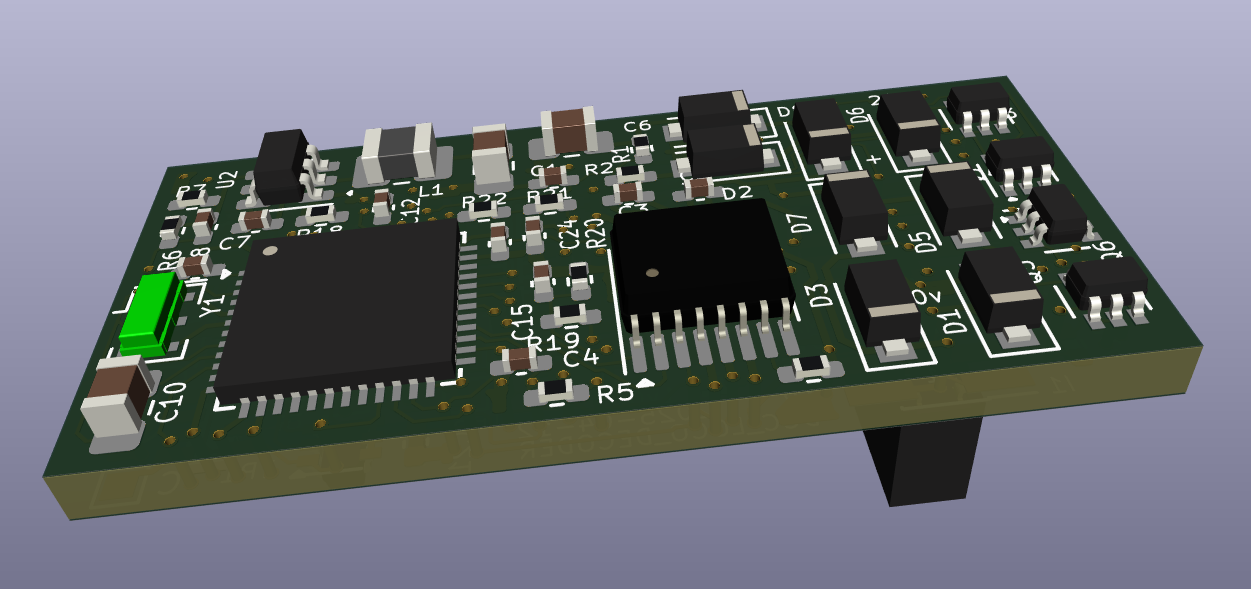
This project wasn't electrically difficult, but it was quite mechanically difficult.
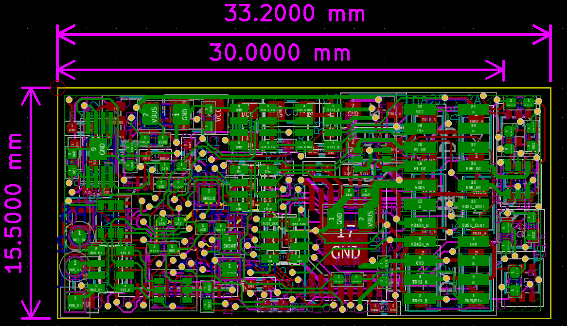
The space allocated for a 21-pin decoder in H0 scale is really small (30mm * 15mm), and I wasn't quite able to fit the design into that space, but it was pretty close - 33.2mm * 15.5mm.
I used primarily 0402 size components in this project (I'd typically use 0603 otherwise), and designed the board with 4 layers.
Microcontroller
After a lot of searching and comparison, I picked the STM32L431 for this project for a few reasons:
- It's got a good amount of flash (256kB) and RAM (64kB)
- Lots of RAM is very convenient for initial development work, as it allows firmware to be downloaded there instead of flash, making the compile/test cycle very quick
- It has a sufficiently fast ADC (5Msps!)
- It's an STM32, which I've used in a lot of projects by now, so I've got a good development environment set up already
- A good number of PWM channels and UARTs
For an unknown reason, I had a few issues using my generic ST-Link devices, but I found using a "real" ST made ST-Link worked without problems.
Something else that caught me out was the way the DMA worked, when using it to read from the ADC. I found I always needed to disable then enable the DMA each time it completed, or it would only work once on boot.
Power
The DCC track input voltage could be as high as 27 volts, appearing as around 26 volts after the bridge rectifier.
As I'm expecting to connect additional modules to this decoder, I decided to use a switching regulator (specifically, the TPS54202).
I've used this in a few projects before, and it's a good fit for the input and output voltages here. One slight thing to be careful of is the EN pin has a max input voltage of 7V, which means that it can't be connected directly to VIN.
A resistive divider needs to be used, with care taken to ensure the voltage is high enough to enable the regulator over the complete range of DCC bus voltages, while not going above 7V for the highest possible DCC bus voltage (replacing R25 with a Zener diode might have been a better idea).
I've also added a small 22uF capacitor to the STM32's VBAT input. Although I've not yet had a chance to see if this works as hoped or not, the aim is to keep the current motor settings and other useful context here, so that if the decoder briefly loses power due to poor track contact, it can resume more quickly when track power is returned.
With a 22uF capacitor, I'd expect the backup domain to keep its settings for around 60 seconds.
There's a GPIO for controlling a "keep-alive" unit, to allow the keep-alive to be disabled during programming.
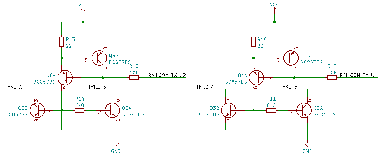
RailCom
This design used the standard RailCom TX circuit, duplicated twice (one for each track input). The two UARTs got mixed up such that UART1 drives RailCom on Track 2 and UART2 drives RailCom on Track 1, but that's easy to resolve in software.
Storage
A DCC decoder will typically need some storage for "Configuration Variables" (CVs), used for setting the DCC address as well as other config options.
As this is a highly experimental project, it needs to be possible to update the firmware without opening up the train to access the decoder.
To make this process easier to implement, I added a small SPI Flash to the board.
This is a 2 MByte device, partitioned as follows:
| Start | End | Length | Notes |
|---|---|---|---|
| 0x00_0000 | 0x03_BFFF | 240kB | Recovery Image |
| 0x03_C000 | 0x03_FFFF | 16kB | Factory Data |
| 0x04_0000 | 0x07_FFFF | 256kB | Update image |
| 0x08_0000 | 0x1E_FFFF | 1500kB (368 sectors) | CV Storage (infrequently changed CVs) |
| 0x1F_0000 | 0x1F_FFFF | 64kB (16 sectors) | CV Storage (frequently changed CVs) |
The mapping of CVs to flash was a challenging one.
Ideally, I would have used an EEPROM allowing individual byte erase, which would have been very simple to implement and probably wouldn't have needed wear leveling at all.
However, I needed quite a lot (~512kB worst case) of space for a factory restore image plus update image, and EEPROMs aren't available in this capacity. Using flash means that changing a single byte might require erasing and rewriting a complete sector, so some kind of wear levelling would be needed.
Storing one CV per flash sector (~4096 bytes) was another option I considered, but rejected as it would have been a very inefficient use of flash, and potentially (if wear levelling was used) been much slower to read on startup.
In the end, I settled on a compromise:
- CVs are grouped into blocks of 24
-
The block number is calculated by dividing the CV number by 24
-
A small header (specifying the first CV in the block, number of CVs in the block and a CRC) is added
- This is written to the start of the sector, if blank
- If the start of the sector is not blank, advance by 32 bytes and try again up to 15 more times (for wear levelling)
- If all 16 'wear level' blocks are used, erase the flash sector and start again
When loading CVs, a very similar approach is used, except that the load routine looks for the last block with a valid header and then loads the CVs from this block.
Some CVs are modified more frequently. A list of these CVs is held in a lookup table, and if a read/write operation is directed to one of them, a very similar approach is used, but with a single CV instead of a block of 24.
Bootloader
The bootloader uses the SPI flash as well.
During runtime, firmware can be written to the update area using the "WriteBlock" commands defined in DCC address partition 253 (see the "Advanced Extended Packet Format" document from the NMRA for more information).
On startup, the bootloader checks this area, and if it finds a new image with correct CRC, it copies it to the STM32's flash and sets a "pending update" bit in the SPI flash.
If the main firmware loaded OK and can communicate with the DCC command station, the command station is then able to clear this pending update.
If the pending update flag isn't cleared after 4 boot attempts, the bootloader considers the update failed, and copies a known-good "recovery image" back to the STM32's memory.
The bootloader also is responsible for setting the flash status register to write-protect the first 256kB of the flash, to ensure the known-good image can't easily be erased.
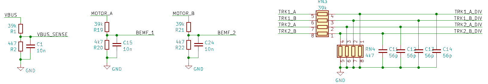
ADC / Input Circuitry
The decoder has 8 analogue inputs on the PCB:
- A "VBUS" sense, which will be the highest out of track 1's voltage, track 2's voltage or the stay-alive capacitor.
- Motor Back EMF inputs 1 and 2 (depending on which direction the motor is turning)
- Motor current sense (from the DRV8874)
- Track voltage sense inputs
- These could be used to determine the polarity and voltage if running in DC mode, or to check for asymetric DCC (used for braking) in DCC mode.
Additionally, a DAC channel from the STM32 is used to generate a variable VREF level for the DRV8874, to set the motor current limit.
If the resistances are too low, then the combined resistor array may overheat, but if they are too high, there's a chance that the inputs might not reliably activate current-based block occupancy sensors.
With this many channels (plus an internal 3.3V rail measurement and on-chip temperature measurement), the ADC needs to run quite fast, especially on the track voltage sense inputs.
The minimum DCC timing, the "1 half bit received duration", is specified as 52us. The ADC sampling time needs to be <26us to sample this correctly, a sampling frequency of 38.4kHz. Multiplying this by 10 channels results in a required sampling frequency of ~384kHz, easily within the ~5Msps ADC sample rate of the STM32L431.
In case of difficulties with using the ADC for the DCC data reception, I also picked analogue channels that had comparators mapped to them as well.
These comparators work well, and I use them for the DCC reception at the moment.
Communication
For a few reasons, the decoder needs to be able to receive messages from other devices.
For example, in a long train model, DCC message reception on the rear unit will be required to resolve the brake section detection issues mentioned in the start.
Also, at some point in the future, I'd really like to model CBTC (Communications Based Train Control), which will likely involve adding an 802.15.4 RF module amongst other accessories.
For this, I'll need some kind of communication bus along the train.
10Base-T1S would almost be a good choice here, but it's still a fairly new technology and the cost (and package size) of a T1S transceiver is quite high, and the required termination at the ends of the bus may be inconvenient to manage.
As an alternative for now, I've settled on a much simpler implementation - an async, half-duplex serial line running the length of the model.
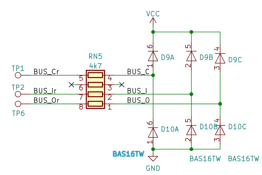
There's a high chance of this pin being shorted to track voltage at some point which means that some robust input protection is required, but the PCB has very little space available. I settled on a 4.7k resistor and some clamping diodes, but I'm not totally happy with this implementation, and I'll probably revisit this again in the future at some point.
A protected RS485 driver like the 65HVD1780 would have been ideal, but these weren't available in the required package size.
In addition to the bus wire, there are "input" and "output" wires, with the intention being to sequentially assign node IDs as trains are joined together (sinc the bus wire will be common to all units).
The SUSI_CLK and SUSI_DAT pins are routed to the 21 pin connector, but I chose these pins to be ones that the STM32 CANBus peripheral was mapped to. As I don't have any decoders which require the SUSI bus, this potentially allows the pins to be reused for CAN.
Conclusion
Basic functionality works!
I've tested the following features:
- Basic DCC command reception
- Bootloader based firmware updates over the DCC track
- Basic function and motor control
- CV reading and writing
There's still a lot to do:
- Properly acknowledging CV writes during programming
- Railcom
- Function flash / blink patterns
- PID (and BEMF) based motor control
- Detection of HLU and ABC braking
As the DCC decoder consists of a microcontroller plus an H-Bridge, it's also possible to use it as a (tiny) DCC command station.
Schematics / PCB: