Overview
This project is nowhere near finished, but as it's taking up a lot of my free time at the moment, I thought I'd add a quick website update in case any of the work-in-progress ideas are useful.
For a long time, I've been interested in processors, and as someone who grew up with various forms of DOS, the idea of building a computer from a very basic level seemed like an interesting project.
When I started pricing up the costs and effort of the project, it was quite difficult to justify for a single CPU - but if I could build a base platform (which would be challenging and expensive) and pluggable processor modules (which would be simple and relatively cheap), the project made a lot more sense.
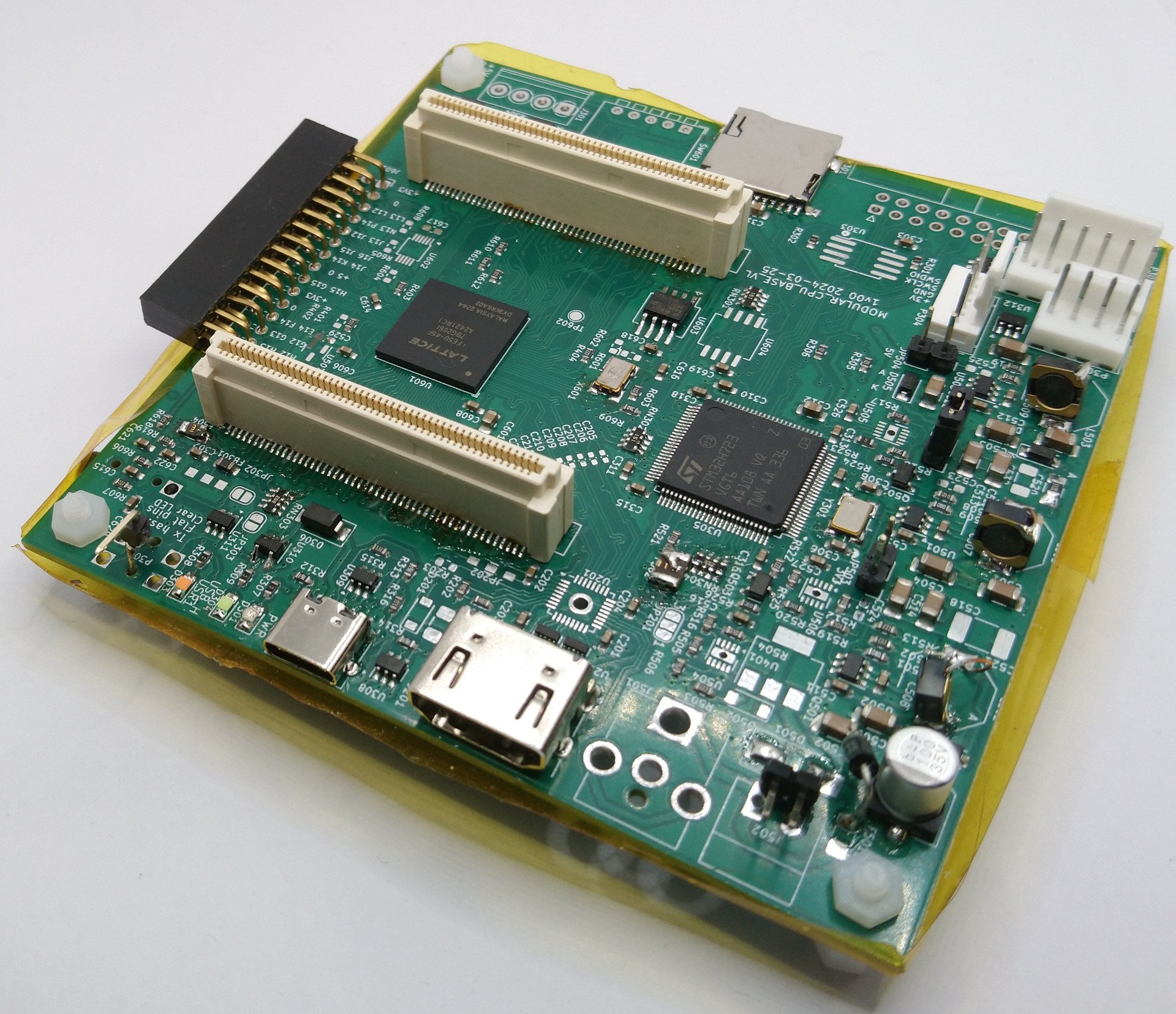
The main board looks like this:
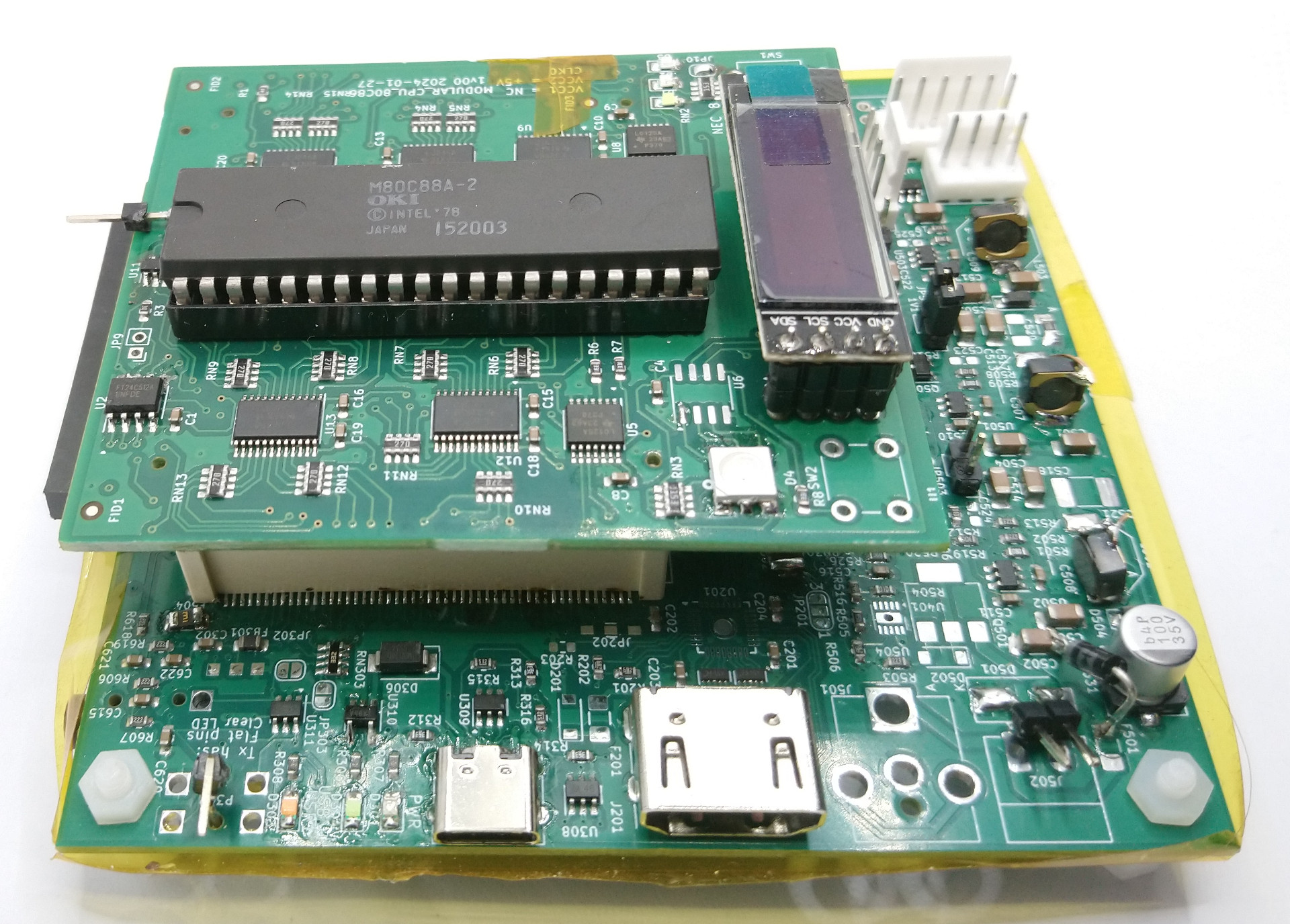
And a complete setup with a main board and 80C86 processor board looks like this:
Main Board
The main board consists of a microcontroller (in this case, an STM32H723) with a QSPI interface to an FPGA (in this case, a Lattice ECP5).

There are also two 0.8mm pitch, 100 pin board-to-board connectors used to connect the processor module. These seemed to be a good compromise between being compact enough to fit within a PC104 footprint, but not having a pitch too small to solder easily, and they also seem to be very widely available from a number of sources.
There are 2x 8MB QSPI RAM devices for a total of 16MB RAM, a very simple RC filter for an audio DAC, HDMI and an expansion connector with 20 usable pins on it, plus 3.3V and 5V.
In use, the board is programmed via the serial configuration interface of the ECP5, but in case it was needed, I also routed the JTAG pins to the microcontroller as well. This works quite nicely for development, as by leaving them Hi-Z in the microcontroller, it's possible to connect an external JTAG cable.
I'm using an Olimex ARM USB Tiny (FT2232H based) adaptor, with the following OpenOCD command line:
openocd -f interface/ftdi/olimex-arm-usb-tiny-h.cfg -c "adapter speed 4000" -f fpga/lattice_ecp5.cfg
Telnet to port 4444, and then run "svf [path to SVF file]"
The board I currently have is a reduced cost version of the original design with a few features removed (no PC104 interface, no Ethernet, 16MB "single channel" RAM rather than 32MB "dual channel" RAM.
This was the first project using a BGA and also first project using the Lattice ECP5 FPGA, so I was slightly nervous about the possibility of getting boards back that were totally non-functional and decided to remove some functionality to allow the board to fit on a much cheaper 4 layer PCB.
As some of the processors may be quite rare or difficult to replace, it's also important that this board has careful control of the power supply rails. This is implemented using SIP32434 power switches, so that voltage rails can be switched on only once the board ID has been read and the safe supply voltages checked.
The processor module design specifies variable voltage rails for VCC2 and VCC_IO, but in this iteration, they're fixed voltages.
Processor Modules
Each processor module has the following:
- 64kB I2C EEPROM at address 0xA8 - 0xAE
- LM75 or eqivalent temperator sensor at address 0x90 to 0x96
- 4x voltage rails: VCC1 (3.3V @ 2A), VCC2 (1.2-5V @ 5A), VCC_EEP (3.3V @ 0.5A) and VCC_IO (1.2V - 3.3V @ 0.5A)
- one I2C Bus
- 106 I/O pins
- 4 Clock nets
Boards may also optionally include other devices on the I2C bus, such as an SSD1306 OLED display, or IO expanders for status LEDs.
Some boards, for example the 8086 board, can accommodate a variety of different processor types (8086, 8088, NEC V20 etc).
As the processor may be in a socket, it's useful to provide the ability to hold a number of board IDs and change between these easily.
To do this, I use the address lines on the EEPROM and LM75 as generic digital inputs like so:
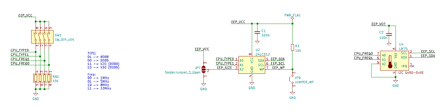
When the microcontroller scans the I2C bus, it will detect an EEPROM at address 0xA8, 0xAA, 0xAC or 0xAE. The microcontroller will then use the detected address to decide which offset to read the EEPROM from - reading starting at 0x0000 if it detected the EEPROM at 0xA8, 0x4000 if detected at 0xAA and so on.
This way, each EEPROM can contain up to 4 images, and DIP switches on the board can be used to select which one is loaded.
These address select lines can optionally be routed to spare data pins on the IO connector.
Processors
I'm planning to build the following processor modules:
| Type | Processor | Status | Notes |
|---|---|---|---|
| x86 | 8086 / 8088 / NEC V30 / NEC V20 | Complete | DIP-40 |
| x86 | 80186 | Not yet started | PLCC |
| x86 | 80286 | Not yet started | PLCC |
| x86 | 80386SX / TI486 | Not yet started | PQFP100 |
| x86 | 80486GX | PCBs ordered, not yet tested | |
| 68k | 68000 / 68010 | Schematic in progress | Will be two separate boards - one DIP, one PLCC |
| 68k | 68020 (QFP) | Not yet started | |
| 6502 / Z80 | PCBs complete, not yet ordered | DIP-40 | |
| MIPS | IDT 79R30x1 | PCBs complete, not yet ordered | PLCC |
Current Status
As mentioned at the start of the page, this project is nowhere near complete!
The main board has arrived and I'm in the middle of the bringup process at the moment (which is looking quite promising so far, apart from an error in the footprint of the SPDIF connector).
I've tested the following functionality:
- USB device
- SD Card
- SWD to the microcontroller
- JTAG to the FPGA from an external JTAG cable
- Microcontroller configuring the FPGA via a bitstream on the SD card
- I2C bus to the processor module
- FPGA DAC outputs
- FPGA SPDIF output (the connector footprint is incorrect)
I've not yet tested:
- HDMI
- USB Host
- Processor Module data pins
- Power switching
I've got the 8086 processor module assembled, and it seems to be mechanically compatible with the main board.
The microcontroller is able to detect the I2C devices on the processor module, but I've not tested more than that yet.
There are a few issues with the main board and the 80C86 module, but nothing major (the READY pin is not routed to the I/O connectors on the 80C86 module, which needs one additional wire adding).
Update 2024-04-17: There's a more significant error on the 80C86 Module.
On Levelshifter U9, the VCCA and VCCB domains are swapped (which is an issue for the 74LVC4245), and the A->B pin is grounded.
Swapping U9 for a 74LVC8T245, isolating the VCCA/VCCB/A->B pins from the PCB, and swapping the supplies while also bridging pin 1 (VCCA) to pin 2 (A->B) is the expected fix.
I plan to publish the Verilog, C and board layouts, but that will take quite some time.
In the meantime, schematics are here:
Main Board schematic: modular_cpu_base_vl.pdf
80C86 Processor Module schematic: modular_cpu_80c86.pdf