Overview
This post is a summary of a display connector standard I defined about 10 years ago.
I'd noticed that a lot of small SPI connected LCD modules used a fairly similar interface (Clock, Data, CS, Reset, and Register select), and thought it would be quite nice if the same connector could be used to support a number of different displays.
It is not the best choice for every application - the main target is for small (320 * 240 * 16 bits per pixel is probably a reasonable upper limit, as a very approximate guideline) LCD or OLED modules with a "4-wire" SPI interface.
The key design decisions I was aiming for were:
- Allows an I2C touchscreen controller (with IRQ) to be used
- Has a good balance of ground wires (for signal integrity) vs pins (aiming for a reasonably small connector)
- Has some level of robustness against reverse connection (by using a keyed connector)
- Allows use of inexpensive connectors and cable (in this case, IDC headers and ribbon cable).
In theory, it might be possible to support autodetection via either an I2C EEPROM or a SPI flash device, but I didn't see many cases where this would be particularly useful. The intention of this standard is to define the hardware interface used on the PCB, and not much more than that.
Definition
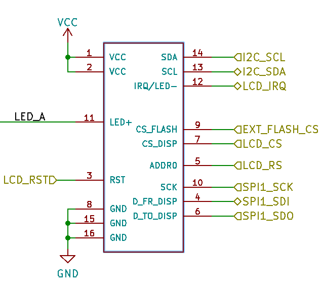
The Common Display Connector is a 2x8, 2.54mm IDC box header, with pins numbered as follows:
| Function | Pin | Pin | Function |
|---|---|---|---|
| VCC | 1 | 2 | VCC |
| RST | 3 | 4 | D_FR_DISP |
| ADDR0 | 5 | 6 | D_TO_DISP |
| CS_DISP | 7 | 8 | GND |
| CS_FLASH | 9 | 10 | SCK |
| LED+ | 11 | 12 | IRQ |
| I2C_SCL | 13 | 14 | I2C_SDA |
| GND | 15 | 16 | GND |
- CS_FLASH is for an optional SPI flash device, and should be pulled high on the microcontroller side if not in use.
- CS_DISP is the display's Chip Select pin
- ADDR0 is also known as DATA/CMD, or Register Select
- D_FR_DISP and D_TO_DISP have been chosen in place of SDI/SDO, to make it less confusing when using the same schematic symbol for both displays and controllers.
- LED+ is a logic level (~10mA max) signal used for backlight control.
- When high, the backlight should be enabled.
Some sample implementations
The first project I can find that used the CDC interface was from 2015 - this was a slightly earlier version of the standard, and it doesn't have an IRQ signal.
Here's an image from a much later project, showing the way this connector might be implemented in a schematic:
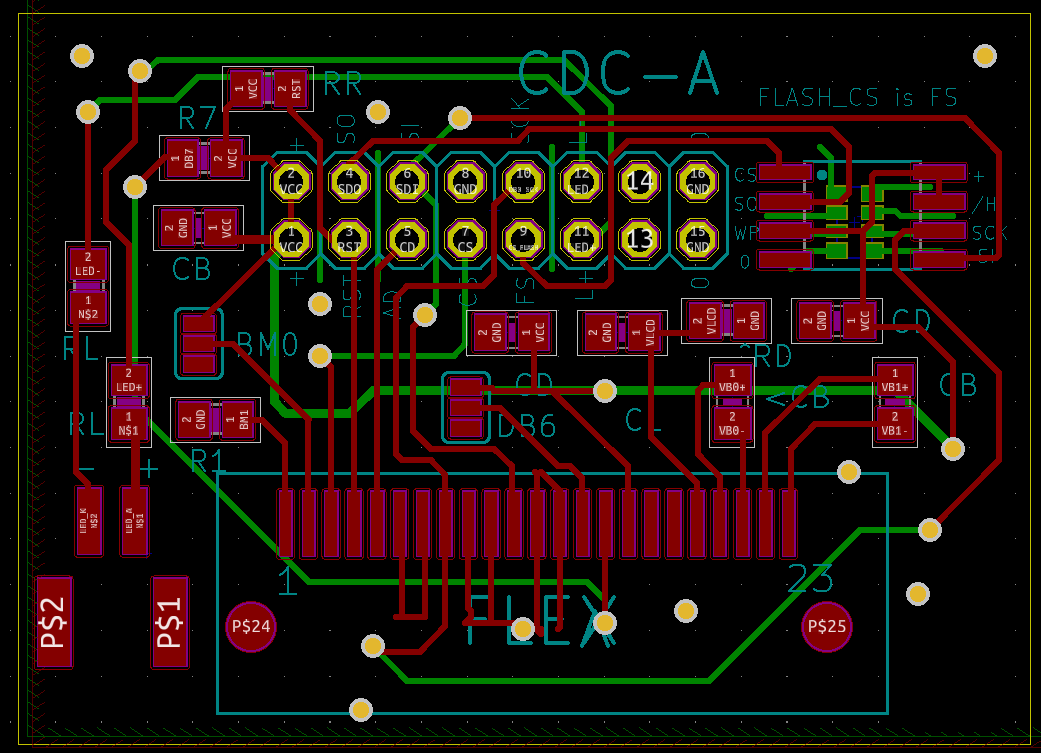
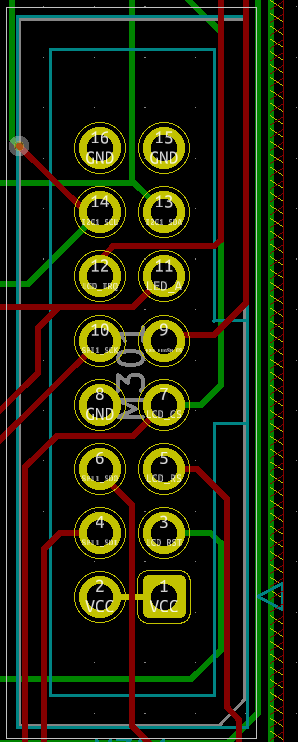
On the PCB, the above schematic looks like this:
Misc
This definition should be considered a public domain work - please feel free to use or adapt it in a project!