Overview
The iD ("Intelligent Device") protocol was a method of connecting multiple devices (typically up to 30) on a single wire.
One example of a device supporting this protocol was the "Karizma" panel from Advanced Design Electronics, but a number of other vendors also supported this protocol (including Texecom and Menvier).
It doesn't seem to be common in new devices, and from reading some comments online it appears that although it was a good idea in theory, it was challenging to work with in practice, especially on longer cable runs.
I'm not considering this to be reverse engineering, as almost all of the required information is in patent GB2423618A, but hopefully this collection of notes might be helpful and more easily found in a search for anyone building their own implementation.
System Implementation
In an iD based alarm system, rather than each sensor being wired to a separate input on a control panel, there's a small device (called a "Biscuit" in documentation) placed into each detector.
Each of these devices has an individual address (presumably set by laser trim at production time or something similar).
This device has three wires - Loop+ (Yellow), Loop- (Blue) and Alarm (White).
The tamper circuit for the detector is in series with the connection from Loop+ to the panel, so that if the tamper circuit is active, the biscuit is no longer detectable by the panel.

This image shows two devices on a single iD loop, but implementations generally permitted up to 30 per loop, with up to 100m of cable for the first generation iD products and 400m on later models.
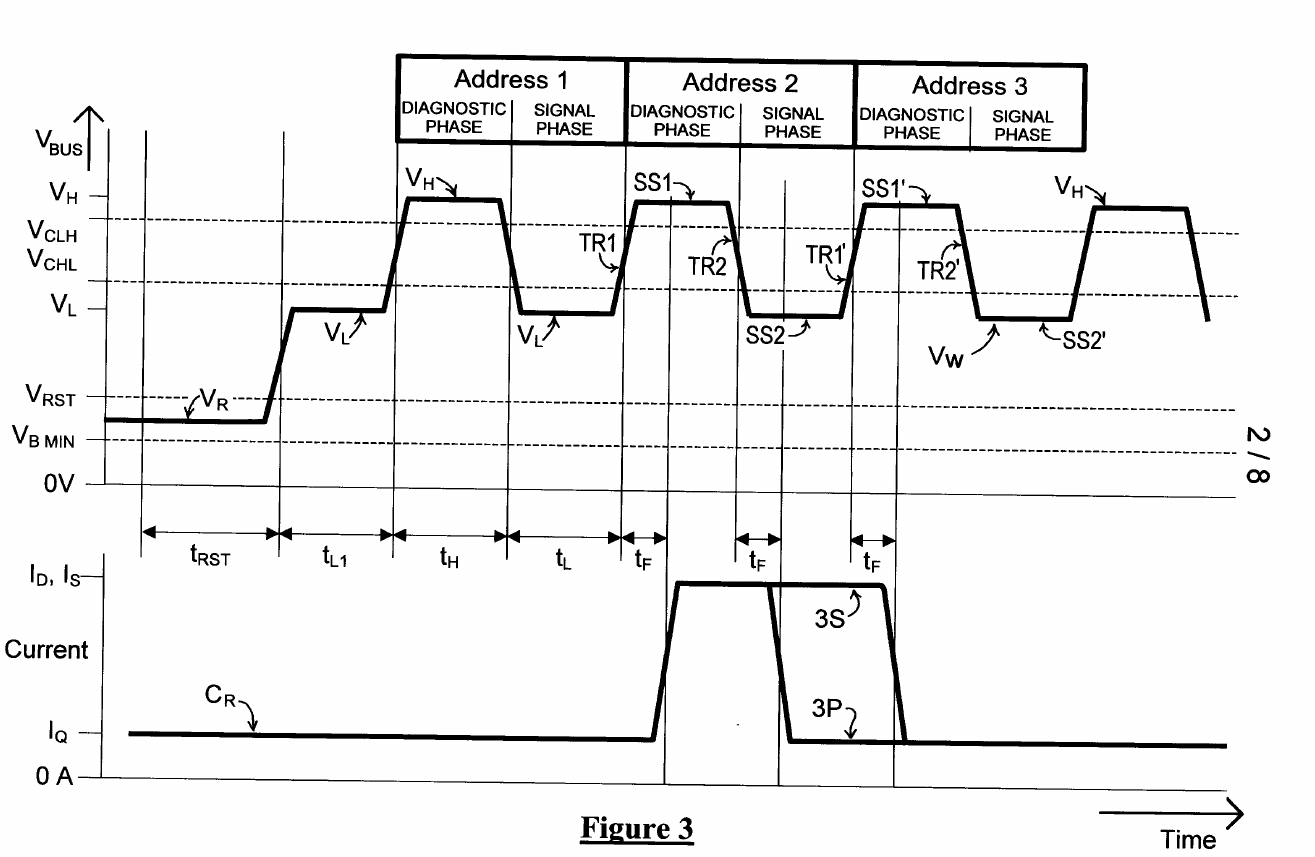
The protocol
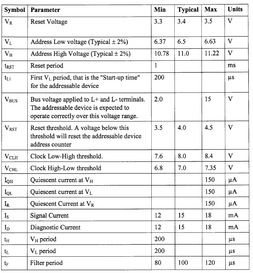
At the start of each detection cycle, the control panel drives the loop voltage to a reset state, VR (3.4V) for time TRST (1ms).
After Trst, the control panel generates a series of pulses (VL=6.5V and VH=11.0V, with duration 200µs in each case).
When an iD biscuit sees the reset voltage, it resets an internal address counter.
Then, on each VH pulse, this address counter is incremented.
Once the address counter matches the iD biscuit's address, the iD biscuit will sink around 15mA during the high part of the pulse (VH), referred to as the "Diagnostic Phase" in the patent documents. Depending on the state of the alarm input, the biscuit may or may not also sink 15mA during the low part of the pulse (VL)
In the patent, this is drawn as follows:
With parameter values as follows:
An Example Implementation
Some very simple proof-of-concept C code is attached at the end of this post to read an iD loop.
This requires a function to set the loop voltage, and a function to read the loop current (although this doesn't need to be in mA).
For this demo, I used an STM32F0, with the DAC driving an opamp to generate the loop voltage, and a current sense resistor (47 ohms) to detect the responses.
This would likely need modification for use in a real / "production" device, but for a demo it seems to work fine.
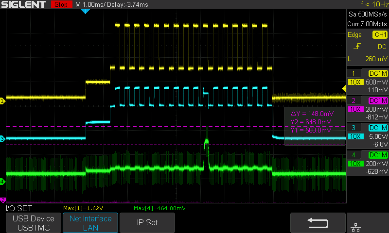
In this waveform:
- Channel 1 (Yellow) is the DAC out of the STM32F0
- Channel 3 (Blue) is the iD line voltage after the sense resistor
- Channel 4 (Green) is the voltage dropped on the sense resistor.
There is an iD biscuit with address 10, and the alarm input closed (shorted to ground -> no alarm).
Useful files
Sample C code to read an iD loop: id_alarm.c