Overview
It's been a while since I posted an update about the modular CPU project - here's the latest status.
Main Board
It can boot DOS!
Not particularly well at the moment - the 8086 board isn't functional at the moment, so I'm using the MCL86 Verilog 8086 core. This works, but it's fairly slow. Booting DOS takes a couple of minutes.
I've been seeing some strange conflicts between the SD card and the QSPI interface to the FPGA - for the initial demos, I've instead just copied the floppy drive image to the SPI flash on the board.
For the BIOS, I've been using a modified version of Sergey Kiselev's 8088 Bios.
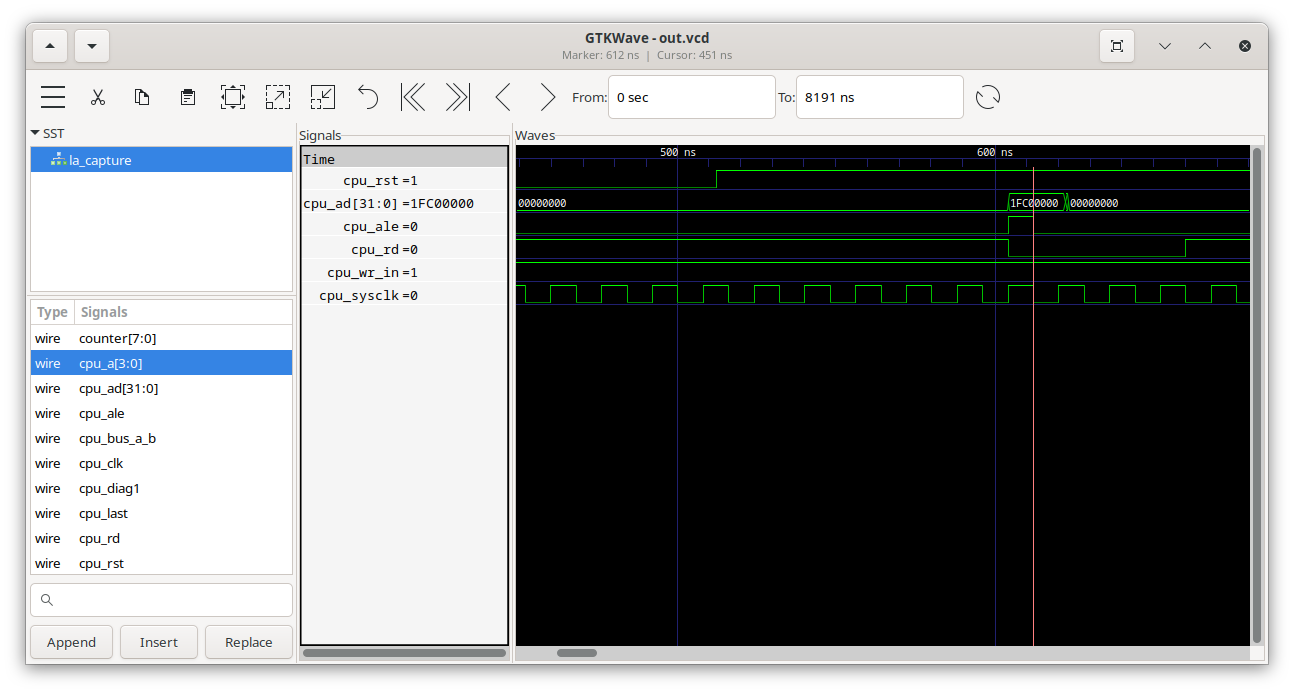
In this bios, I've rewritten the INT13 (disk IO) routines as follows:
- When INT13 is called, copy all of the function parameters to the IO space from 0x050 to 0x05F (this space is mapped to a small dual-port RAM on the FPGA)
- Set a "request pending" flag for the STM32 by writing the interrupt number (0x13) into another IO port (0x05D)
- Once this is done, the clock to the 8086 is stopped, and the STM32 receives an interrupt
- The STM32 will then read from this dual-port RAM, run the corresponding INT13 routine (which may read a sector from the floppy disk image on the SD card, and copy it to the location specified in the INT13 handler)
- If the 8086 is paused, the STM32 has read/write access to the entire system IO and memory space
- If the 8086 is not paused, the STM32 has no access to the main IO and memory spaces, but does have access to the small dual-port RAM
- Once the STM32 has finished, it clears the "request pending" flag, which allows the 8086 to resume, and writes a status code to indicate if the INT13 request failed.
- Depending on the value in IO address 0x05C, the 8086 will copy back either AH/AL, or all relevant registers
This modified file can be found here: modular_cpu_x86_int13.txt
Additionally, there's a keyboard input driver on the STM32. Once a USB HID report has been received, the STM32 uses a lookup table to map this to an XT keyboard scancode.
This value is then driven into the 8255 on the FPGA, in the same way that it's driven by a shift register for the keyboard on the IBM XT (although it would benefit from a FIFO, as it drops key presses quite easily at the moment).
USB HID to XT Keyboard scancode mapping (very incomplete for the moment, but works well enough to navigate around DOS):
8086 Board
This board has quite a few issues.
- The "Ready" signal is not driven by the FPGA
- The "TX Enable" signal is not driven out to the FPGA
- The data direction for U9 is incorrect - this should be tied high.
- The silkscreen indicates that DIP switch 2 selects the CPU bus width - it should be DIP switch 1.
- I strongly suspect that the TX enable control should have been connected to DEN, rather than DT/R.
- The supply domains for U9 are incorrect
However, as I've got 10 of these boards (assembled), it makes sense to try to use them, so:
- The lv_ready signal on pin 5 of U2 can be connected to a spare pin on the module connector
- The TX enable pin can be connected to a 74LVC1G gate, to reduce it to 3.3V, and then connected to another spare pin on the module connector
- The VCCA supply to U9 can be disconnected and reconnected to 3.3V. Pin 2 can be lifted from GND and connected to pin 1 (now 3.3V)
- Note, this isn't ideal - these pins would ideally be at +5V rather than +3.3V
- The pins on the DIP-40 socket for DEN and DT/R are adjacent, so if the DT/R pin is removed from the socket, it can be bridged to DEN on the PCB
486GX Board
This board is able to boot as far as the BIOS, but seems to be failing memory tests in the first 64K of RAM, although not at a consistent location.
During the initial bringup of the main board, the LDO I was using for the 2.5V supply on the FPGA didn't seem very close to 2.5V.
I've since replaced that LDO, but I've not yet had a chance to retest the 486 board to see if it's improved the reliability or not.
68K Dragonball Board
This board has a one annoying design issue - the 32kHz clock from the FPGA is connected to the crystal driver output, rather than input.
Some of the bus width selection logic on the board is not ideal (the jumper for selecting a 8 or 16 bit databus width isn't usable, but this isn't a major issue as the pin is also connected to the FPGA, providing R7 is reduced from ~10k to ~100 ohms). This also needs to be done to use this pin as the 68k DTACK signal.
I've not yet tested the SDRAM on the board (although, in retrospect, it would have been nice to have arranged the data pins on the SDRAM to allow either an 16-bit or 8-bit part - the current schematic only allows a 16-bit RAM).
Apart from that, I've been able to run a few instructions on it, mostly just verifying that the address and data pins are connected correctly.
MIPS IDT79R30x1
Not properly tested this yet, but the first board is assembled!
There are a couple of minor issues (that should be possible to work around), but it functions enough to fetch the reset vector at least: