From time to time I like building retrocomputing projects based on old CPUs, and I decided that the 68K would be a fun challenge.
The "DragonBall" is a very interesting SoC based around a 68000, with some useful peripherals added:
- IRQ controller
- 2x UARTs
- 2x SPI ports
- LCD controller
Additionally, it's a 3.3v part and has an internal bootloader ROM (this is very helpful, as it means that SMT Flash chips can easily be used).
This project was a PC104 CPU card based around the DragonBall VZ ( MC68VZ328P ), plus the following:
- USB -> UART bridge (based on an STM32F042) that allows resetting into the bootloader
- CAN-FD interface (based on MCP2517FD)
- 512k * 16 bit PSRAM
- 16M * 16 bit Flash
- ICE40-UP5K FPGA for a PS/2 keyboard and mouse, plus VGA video out.
Unfortunately, getting a working 68K toolchain was probably the most challenging part of this project (and also the least interesting).
Details:
PCB:
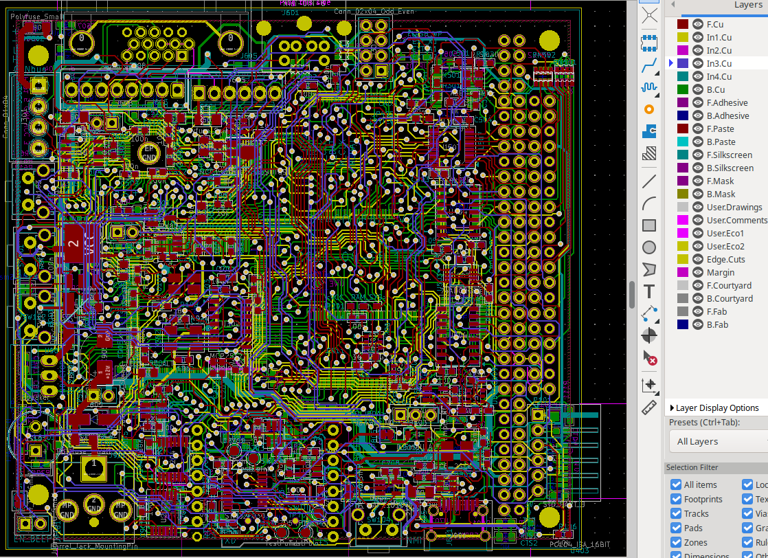
I tried routing this on a 4 layer PCB, but found I needed to switch to a 6 layer board to route the 24 bit address and 16 bit data busses around the board (they need to route between the CPU, RAM, Flash and PC104 connector).
This was my first 6 layer board (and I switched to 6 layers fairly late in the layout stage), so I'm not sure the layer stackup here is optimal, but it is:
- Top : Signal
- In1 : Signal
- In2 : Ground
- In3 : Signal
- In4 : Power
- Bottom: Signal
This board was designed in KiCAD.
Memory Map:
The 68000 has only 24 address pins, but the CS generation logic is on-chip, connected to the 32 bit address bus. For this reason, there's more than 16MB of accessible space on the board.
0x0000_0000 - 0x03FF_FFFF -> ROM (CSA0)0x0400_0000 - 0x07FF_FFFF -> System RAM (CSA1)0x0800_0000 - 0x0BFF_FFFF -> User RAM (CSB0)0x0C00_0000 - 0x0FFF_FFFF -> User RAM (CSB1)0x1000_0000 - 0x13FF_FFFF -> ISA (8 bit) (CSC0)0x2000_0000 - 0x23FF_FFFF -> ISA (16 bit) (CSD0)0xFF00_0000 - 0xFFFF_FFFF -> SFRs
PC104 interface
This bridges the 68K bus to the PC104 (ISA) bus.
CSC0 is used to select an 8 bit access, and CSD0 is used to select a 16 bit access (I'm not certain, but I think the 68000 doesn't support the peripheral determining the access - so this must be determined by the CPU instead).
Unfortunately, I misunderstood a comment in the datasheet, so the upper and lower bytes going to the PC104 interface are swapped!
A23 is used to select between a memory access and an I/O access, as the 68K does not support a separate IO space. The 64K ISA address space is aliased multiple times in the range 0x1000_0000 to 0x13FF_FFFF and this duplication is used to generate a variable number of wait states, depending on the address selected.
For example, an access to 0x1000_0010 will access ISA IO address 0x10, with 0 additional wait states.
An access to 0x1020_0010 will also access ISA IO address 0x10, but with one additional wait state (and 0x1040_0010 would access the same location with 2 wait states).
Additionally, the ISA WAIT signal is included in the DTACK generation logic, so any card requiring more wait states can request them.
Note that the DragonBall is configured to only sample the DTACK pin for accesses to the ISA space - internal ROM / RAM accesses do not check DTACK (instead using a fixed number of wait states, generated on-chip).
UPDATE 2023-11-25 : While bringing up another PC104 project, I found there are two errors in the PC104 read/write enable logic.
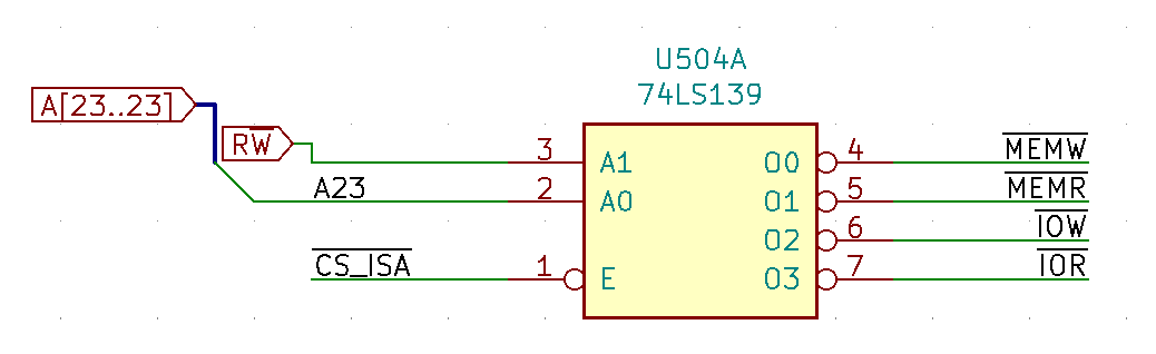
The first error is the ordering of A0 and A1 on U504A. RW should be connected to the A0 input.
Additionally, the Dragonball is not easily able to generate the chip select signal for 16MB blocks of address space that isn't DRAM.
The largest usable chip select area is 4MB, so I had to connect the system address line A21 to pin 3 (A1) of U504, and the R/W signal to pin 2 (A0).
Once this was done, the PC104 card I was testing worked OK, although I've not yet tested interrupts.
DTACK Generation
Here's a more detailed view of the DTACK generation logic:
"RST_DTACK" is the NAND of the ~UD and ~LD signals. This ensures the shift register is held in reset when no memory access is happening.
Once a memory access happens, the shift register (which has a '1' on its input pin) begins to shift on each positive edge of the CPU clock.
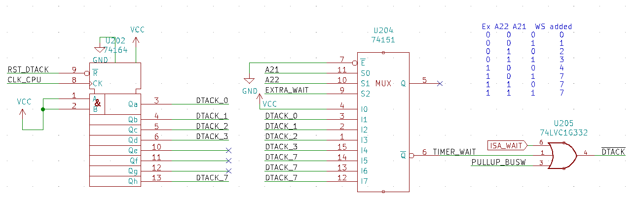
U204 is a mux, controlled by two address lines plus a GPIO pin, which allows one of the shift register outputs to propagate to the DTACK pin (Shift register outputs 4, 5 and 6 aren't used - this was just due to PCB routing constraints making it very difficult to get them from the shift register to the mux).
Also note that on the DragonBall, DTACK is used to set the width of the memory used at startup, needing to be pulled high on reset for 16 bit memory.
Interrupts are OR'd together to reduce the total number of interrupt pins required, and ISA DMA is not supported.
USB -> UART interface
This is based on an STM32F042, to implement a very slightly custom UART interface (to allow interacting with the BOOTSTRAP pin required to enter the bootloader).
I could probably have connected RTS to BOOTSTRAP and DTR to reset and used an off the shelf USB -> UART IC, but I had the STM32F042s available from another project and it also allows for future development.
The STM32F042 is running a very slightly modified copy of ST's USB->UART demonstration, with a modification to look for an incoming BREAK over the USB interface. When a BREAK is seen, the next character is checked:
- N -> Generate an NMI
- B -> Assert BOOTSTRAP, generate a reset (to restart into the ROM bootloader)
- R -> Deassert BOOTSTRAP, generate a reset (to restart into the user program in ROM).
To work with the onboard bootstrap loader, I developed bootstrap.py. This allows memory testing, along with downloading a program into RAM and running it.
The onboard boot ROM on the dragonball allows writing to memory and running 68K instructions, but it doesn't seem to allow memory reads.
I implement memory reads with a tiny 68K program (generated with python string substitution!) which copies the byte into D7, and then moves D7 into the UART.
This program gets copied into the bootstrap's instruction buffer, and then run:
#Tiny 68k program to read a byte into the UART:
# move.b ($<loc to read>), D7 : 1E39 <4 byte addr>
# move.b D7, ($<UART BUFFER>)) : 13C7 <4 byte addr>
# jmp $FFFFFF5A ;back to bootloader : 4EF8 FF5A
read_prog_len = 16
read_prog = "%08X%02X1E39%08X13C7%08X4EF8FF5A\r\n" % (
self.INSTR_BUFFER, read_prog_len,
addr, self.UART1_ADDR
);
self.port.write(str.encode(read_prog))
data_back = self.port.read(44)
self.port.reset_input_buffer()
self.go(self.INSTR_BUFFER)
Note that if running at higher baud rates, using RTS/CTS handshaking is highly advised.
SPI Devices
Not too much to say here - there's an MCP2517FD CAN-FD controller, plus a MicroSD card in SPI mode. The FPGA (for video output) is also connected via SPI.
UARTs
One UART is connected to the onboard STM32. The other UART is connected to a pin header, plus an IRDA module.
Memory
RAM
The RAM is a fairly conventional 512k * 16 bit PSRAM (excluding some slightly odd connection of the memory address pins, in order to support both 256k and 512k RAMs).
The CS logic on the DragonBall is able to tell the difference between a 68K user mode and supervisor mode access, so I used CSA1 for supervisor accesses, and the CSB0/CSB1 for user mode accesses (although I've not tested this feature yet).
The idea here was to allow implementing a preemptive multitasking OS with memory protection, although I've not yet fully checked this functionality.
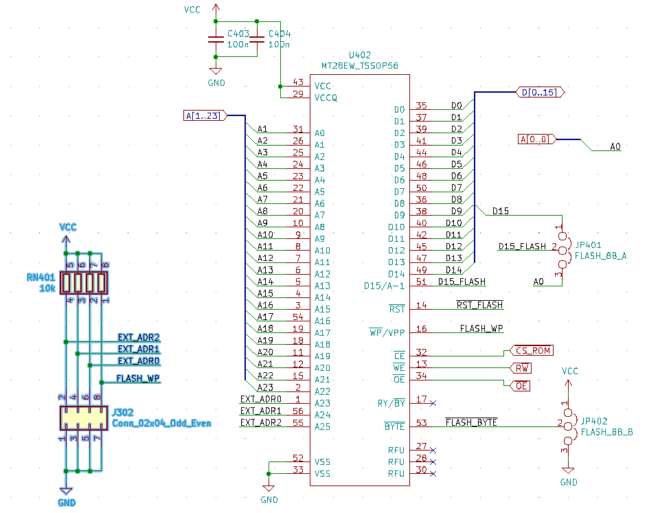
Flash
I had a few MX29GL256F parts, which are 16M * 16 bit Flash chips. These are the largest flash size that can easily be supported on the board, due to the 23 address lines.
However, I did also see some higher capacity NOR flash devices, so to allow these to be used as well, the additional address pins are connected to jumpers. This means larger flash devices can be supported (although only a maximum of 16MB is accessible at one time).
The board is also designed to accommodate either 8 bit or 16 bit flash by means of jumpers JP401 and JP402.
VGA interface
The DragonBall has an LCD controller, designed for driving controllerless LCDs.
This controller generates DMA transfers from a programmed location, and serialises this over 1/2/4/8 data lines.
On this project, I routed 4 of these data lines (plus the bit clock / frame start signals) to an ICE40-UP5K FPGA. This FPGA also has an RGB333 video output, PS/2 keyboard and mouse, footprint for QSPI RAM and provision for a 1-Wire interface.
It's connected to the CPU via SPI, plus two interrupt pins.
Current status:
This project is on hold for the moment, for a few reasons.
Getting a working C toolchain was a really challenging part of the project (I spent about a week debugging crashes when using variadic functions), and it's not possible to trace line-by-line on this board.
I also designed this board during the parts shortage in 2021, which meant that many of the ICs weren't available at the time the PCBs returned from fabrication, which further delayed the project.
In the event that it's useful, I've attached a ZIP of the schematics, header files and bootstrap loader script: pc104_dragonball.zip
There are a few known issues (particularly on the PC104 bus!), and I've not yet evaluated all of the functionality of the board - please consider this a source of possible ideas, rather than a finished project!